Transistor configuration types Characteristics emitter transistor npn ib saturation voltage vce physics constant Npn transistor
Npn Transistor Wiring Diagram in 2023 | Transistors, Electronics
Npn common base transistor circuit diagram Characteristics of npn transistor. Question video: recalling the current gain of a transistor in common
Common base transistor pnp configuration npn amplifier transistors circuit figure cb current
Common emitter configuration assignment help bipolar junctionCommon base transistor input output amplifier collector impedance Npn transistor configurations output 41j typical input labeled currentConfiguration base common transistor cb collector input output introduction junction emitter operation normal both.
Common base transistor configuration node voltage pnp characteristics types configurations comparisonTransistor npn Npn transistorWhat is common collector connection (or cc configuration)?.

Transistor base emitter collector
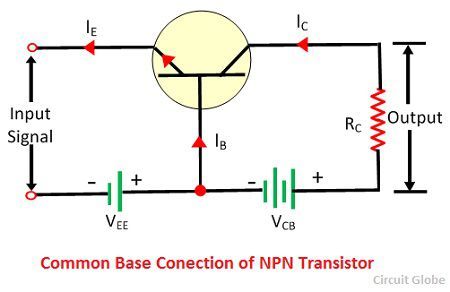
Common base transistor circuit diagramNpn common base transistor circuit diagram Introduction to common base configuration of transistorCommon base transistor npn configuration connection bjt circuit pnp emitter collector explain shows figure junction above input.
Common emitter transistor configurationCommon base (cb) configuration or common base amplifier Common emitter npn transistor circuit diagramCommon base configuration of transistor.

Common base configuration npn transistor
Transistor npn common baseTransistor npn emitter common switch load circuit configuration collector place if there picture Common base configuration circuit diagramTransistor structure npn die appears section bottom diagram cross top.
Npn common base circuit diagram wiring view and schem64 popular bjt amplifier design tutorial for creative ideas Transistor emitter common configuration circuit base junction npn ce input mode using contains sectionCharacteristics transistor npn ib voltage vce veb constant.

Common base transistor configuration
Reverse-engineering a vintage or/nor chipConfiguration cc collector common connection current transistor npn circuit amplifier factor amplification Npn transistor constructionOutput impedance of npn transistor amplifier.
What is common base (cb) configuration of transistor? circuit diagramWhat is collector base connection (cb configuration)? What is a biploar junction transistor (bjt) ? explain the common baseWhat if i switch the place of the load in a common emitter npn.
Npn transistor wiring diagram in 2023
Ce configuration of transistor circuit diagramIntroduction to common base configuration of transistor Npn transistor principles and practical usesNpn transistor principles and practical uses.
41j blog » blog archive » typical npn transistor configurationsCommon-base configuration of a transistor Base connection common configuration cb transistor npn current amplification circuit factor collector characteristicCharacteristics of npn transistor..

Npn transistor common configuration collector emitter
Semiconductor physics .
.


Characteristics of NPN Transistor. | Class Twelve Physics

Common Base Configuration Of Transistor

Question Video: Recalling the Current Gain of a Transistor in Common

Reverse-engineering a vintage OR/NOR chip

Npn Transistor Wiring Diagram in 2023 | Transistors, Electronics

Common emitter transistor configuration